


Protocol Reference Manual
Introduction
The Baseboard is a FPGA-based robot or automation controller that has an FPGA for logic, timing, and I/O pins, and a USB-serial interface. The USB serial interface connects to a host computer that controls the peripherals implemented in the FPGA. This document describes the protocol between the host and FPGA.
The peripherals in the FPGA are each given an /address/ that uniquely identifies a peripheral instance. Each instance of a peripheral has a set of 8-bit /registers/ which control the peripheral. This document describes all of the DPI peripherals and their associated 8-bit registers.
The intended audience of this document includes programmers and engineers who wish to build custom interfaces for peripherals on the FPGA card.
Overview
Figure 1 shows the overall architecture of the system. Applications connect over TCP to a daemon (called /pcdaemon/) that converts the high level commands from the user to the low level register reads and writes in the FPGA to implement the command. For example if an application uses pcset to set a PWM pulse width to 55 percent it is pcdaemon that converts "55 percent" to the proper 8-bit register values to control, for example, the clock prescaler and period counter. Pcdaemon also manages the communication with FPGA and forwards sensor reading to applications that have used pccat to subscribe to the sensor.
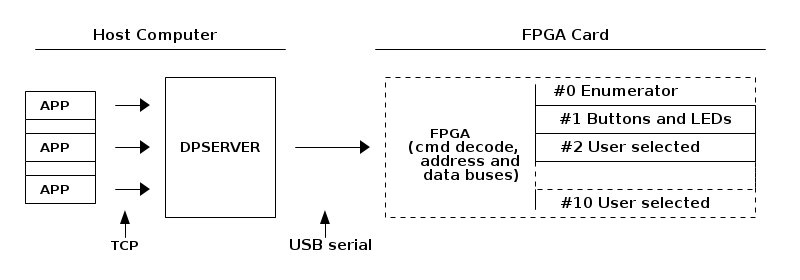
The BaseBoard4 FPGA card supports up to eleven different peripherals. Of the eleven peripherals, nine, Peripheral #2 through Peripheral #10, are defined by the user (customer) and two, Peripheral #0 and #1 are included in every build of the FPGA firmware. Peripheral #0 refers to an internal read-only memory, called the enumerator, that containing a list of the peripherals built into that specific FPGA image. When the Linux daemon starts, it reads the contents of Peripheral #0 and configures itself to match the peripherals it finds listed in the enumerator. Every build of the FPGA image has an enumerator and it is always at Peripheral #0. Another peripheral included in every FPGA image is Peripheral #1 which manages the eight LEDs and three buttons on the BaseBoard4.
Protocol Specification
Features of the protocol include the following:
-
The protocol is organized as SLIP encoded packets
-
Each packet contains either a Read or Write command
-
A packet may read or write multiple values
-
A packet may read or write the same register or consecutive registers
-
Registers are 8 bits wide
-
Addresses are 16 bits with one byte for peripheral address and one for the register address. The peripheral address is 5 bits in length and the high 3 bits are set to one. Note that the protocol has a 13 bit address even though the FPGA only uses 12 bits.
-
A response packet indicates success or failure of a command packet
-
Data can be sent automatically from the FPGA to the host
Packet Format
Commands to the FPGA and responses to the commands are sent as SLIP encoded packets. Each packet is composed of a command byte, an address byte, a register byte, a transfer count byte , and, if a write command or a read response, the data bytes. All command responses include the original command byte, the 16 bit address, and the transfer count. Responses also have a byte after the transfer count that indicates how many words remain to be transferred if there are additional response data words remaining to be sent. (Getting the number of bytes written or read is useful when dealing with FIFOs.) A command packet from the host to pccore has the following format:
Byte |
Meaning |
SLIP End Char |
|
Command Byte |
Read or Write with/without auto-increment |
Peripheral ID |
Peripheral or slot # (111x xxxx) |
Register Address |
Start address if auto-increment |
Request Count |
Number of bytes requested |
Data |
|
:::: |
|
Data |
|
Transfer Count |
Only on read response |
SLIP End Char |
Serial line devices (such as the FTDI USB-serial chip) often drop characters when overloaded. Using SLIP encoding helps limit the loss to a single command when characters must be dropped.
Serial Line Internet Protocol (SLIP) encapsulation is described by RFC 1055. SLIP packets end with an END character (0xC0). This implementation of SLIP uses Phil Karn’s extension which starts packets with an END character. In a packet the END character is replaced by the two byte sequence 0xdb, 0xdc. The character 0xdb is defined as the ESC character. In a packet the ESC character is replaced by the two byte sequence 0xdb, 0xdd. It is a protocol violation to have an END character appear anywhere in a packet. It is also a violation to have an ESC character that is not followed by either 0xdc or 0xdd.
The first byte in the packet is the command that tells the direction and type of command. Of the 256 possible values for the command byte only six are used:
0x44 : auto-send from FPGA to host from a single register |
||
0x46 : auto-send from FPGA to host from auto-incrementing registers |
||
0xf4 : read from a single register |
||
0xf6 : read from auto-incrementing registers |
||
0xf8 : write to a single register |
||
0xfa : write to auto-incrementing registers |
The second byte in the packet has the 5-bit peripheral address. This address implicitly specifies which FPGA and connector pins are associated with the peripheral. While generally consecutive, peripheral addresses do not need to be. For example, a peripheral that spans eight FPGA pins also spans two peripheral addresses. The third byte specifies which register in the peripheral to read or write. If the command is for a multi-byte transfer with incrementing register addresses, the third byte specifies the starting register number. The fourth byte specifies how many bytes to transfer. Up to 255 bytes can be transferred by a single command.
The packet format described here is used for all commands to the FPGA. Response packets from the FPGA add one more byte after the data. This byte indicates how many bytes remain to be transferred. Usually the transfer count is zero, indicating that all bytes were transferred. However, when reading or writing to FIFO-based peripherals you might not know beforehand how many bytes are queued for sending. In this case it is best to send read requests with a request count of 255 and the peripheral can send bytes until it exhausts its queue. How many bytes are in the read response can be verified as 255 minus the value of the transfer count. Writing data to a FIFO is similar. Send a write packet with as many words as you wish, but watch the transfer count in the response to see if the peripheral had to drop part of the data you sent. Use the transfer count field to compute which data needs be resent in a later write packet.
Many systems require that the host poll peripherals for new data. This type of polling can place a heavy load on the host processor and can severely limit data rates to and from the peripherals. Our design allows peripherals to respond to an external event by automatically building and sending a read response packet to the host. The command byte is 0x46 or 0x44 for packets sent automatically by the FPGA. Peripherals can send a packet up to the host at most every 4 milliseconds. A typical aggregate data rate for a peripheral sending a packet every 4 milliseconds is on the order of 2500 bytes per second. Please contact Demand Peripherals if your application requires an FPGA image build with an update rate faster than every 4 milliseconds. It is easy to change but there may be some design trade-offs to consider.
A Demand Peripherals Protocol Testbed
The pcdaemon source code has two C programs that can help you explore the registers and peripherals the system. The first program, pcdump, displays packets sent from the FPGA to the host. It removes the SLIP encoding and displays each packet byte as a two digit hexadecimal number. The whole packet is displayed on one line and a newline separates consecutive packets.
A typical sequence to compile and run pcdump might be:
gcc -o pcdump pcdump.c
/pcdump /dev/ttyUSB0 &
Install pccore.bin using the following sequence.
sudo chmod 666 /dev/ttyUSB0
stty -opost < /dev/ttyUSB0
cat pccore.bin > /dev/ttyUSB0
Peripheral #1 is always tied to the LEDs and buttons on the FPGA card. The buttons on the BaseBoard4 are edge sensitive and automatically send updates to the host on a button press or release. If you have loaded and are running pcdump a press of button 3 should give a packet dump of: 01: 46 01 00 01 04 00
As a reminder, 01: is the board number, 46 is the command byte, 01 is the peripheral address, 00 is the register address, 04 is the value assigned to button 3, and the final 00 indicates that all (one) of the requested registers are being returned in this packet.
The other program, pcxmit, SLIP encodes a packet for transmission to an FPGA card. Build and run pcxmit with the following commands: gcc -o pcxmit pcxmit.c ./pcxmit >/dev/ttyUSB0
The input to pcxmit is a line of hexadecimal numbers separated by spaces. Each line is send as a complete SLIP encoded packet. The LEDs are accessed as a byte write to register 1 at peripheral #1 (or address 0xe1 since the high 3 bits are one). The packet to set the LEDs to 0x55 would be: fa e1 01 01 55
The above packet generates the following response from the FPGA 01: fa e1 01 01 00
Peripheral and Register Definitions
This section gives the low level register definitions for a few of the peripherals offered by Demand Peripherals. The reader is assumed to have sufficient background in programming and electrical engineering to find the register definitions sufficient.
The peripherals are listed alphabetically.
BB4IO: BaseBoard4 Buttons and LEDs
The BaseBoard4 FPGA card has three buttons and 8 LEDs on the card. Collectively these are the BaseBoard4 I/O peripherals and are always at address Peripheral #1. An 8-bit read of Peripheral #1, Register 0 returns the current status of the buttons. The state of button 1 is in the LSB, button 2 is in bit 1, and button 3 is in bit 2. A set bit indicates that the switch is closed. The button inputs are edge triggered and a press or release of a button automatically sends a read packet response (cmd = 0x46) to the host. You do not need to poll the buttons to get a press or release event. An 8-bit hexadecimal write to Peripheral #1, Register 1 sets the LEDs. Bit 0 of the byte sent controls the bit 0 of the LEDs. A set bit turns on the LED. A read of Register 1 returns the current status of the LEDs as an 8-bit value.
Register |
Meaning |
Register 0: |
Button status |
Register 1: |
LED control & status |
Enumerator
The enumerator is a block of read-only-memory which describes the peripherals in the FPGA image. The pcdaemon program uses this information to configure itself when it starts. This ROM also contains a copyright notice, the email address of the person who accepted the license, and the date of the build.
The ROM is organized as a list null-terminated ASCII strings. The first eight strings contain licensing information and the rest of the strings contain the list of peripherals in the build.
The ROM has at most 2048 characters and is always Peripheral #0. The enumerator has a single 8-bit register that is accessed as a FIFO. Typically you would read the ROM by issuing a series of 8-bit reads of 255 words from register 0. An internal counter keeps track of the reads so that subsequent reads pick up the next character to send. You may reset the internal counter by doing any 8-bit write to register 0. The data written is ignored.
The information in the enumerator is broken into strings of text with the following meaning assigned to each string.
Register |
Meaning |
String 0: |
Copyright |
String 1: |
Licensee email address |
String 2: |
Build date |
String 3: |
(unused) |
String 4: |
(unused) |
String 5: |
(unused) |
String 6: |
(unused) |
String 7: |
(unused) |
String 8: |
enumerator (slot #0) |
String 9: |
bb4io (slot #1) |
String 10: |
Peripheral_slot_2_name |
String 11: |
Peripheral_slot_3_name |
String 12: |
Peripheral_slot_4_name |
String 13: |
Peripheral_slot_5_name |
String 14: |
Peripheral_slot_6_name |
String 15: |
Peripheral_slot_7_name |
String 16: |
Peripheral_slot_8_name |
String 17: |
Peripheral_slot_9_name |
String 18 |
Peripheral_slot_10_name |
The enumerator and BaseBoard4 I/O peripherals (Buttons and LEDs) are always assigned to slot zero and one. The string peripheral_slot_x_name above is replaced by the name of the library for the peripheral the user has selected for that slot. Examples of typical library names include "dc2", "quadrature2", and "servo4". Each slot has four pins associated with it. Some peripherals can use eight pins, not four, and we need a way to indicated that a slot is unused or is used by the previous eight-pin peripheral. A special peripheral named "null" fills this need. A null peripheral takes four pins but does not actually have any registers associated with it.
GPIO4: Quad General Purpose I/O
The Quad General Purpose I/O peripheral provides four FPGA pins for either input or output. When configured as an input, each pin may additionally be configured to send up to the host the new value of the input when the input changes.
The GPIO4 peripheral has three 8-bit registers located at addresses 0, 1 and 2. A read of Register 0 returns the current values at all four pins and a write sets the values for those pins configured as outputs. Bit 0 in each register corresponds to the lowest numbered pin on the BaseBoard4 connector. Register 1 is the direction register with a one indicating an output and a zero indicating an input. All four pins default to inputs after power up. Register 2 is the interrupt-on-change configuration register. Here an "interrupt" refers to asynchronously sending to the host a USB packet that contains the most recent values available at the pins. Setting a bit to one enables interrupt-on-change for the corresponding pin. The power up default is to turn off interrupt-on-change. A change on an interrupt enabled pin causes the peripheral to send to the host a read response packet for a read of one 8-bit register starting at register 0.
Register |
Meaning |
Register 0: |
Read: Current values of all pins |
Write: Sets the output pins |
Register 1: |
Direction: Output if 1. Input if 0 |
Register 2: |
OUT4: Quad Output Peripheral
The Quad Output peripheral provides four FPGA pins for simple binary output.
The OUT4 has one 8-bit register at address 0. A read of Register 0 returns the current values at all four output pins and a write sets the pins. Bit 0 in the register corresponds to the lowest numbered pin on the BaseBoard4 connector.
Register |
Meaning |
Register 0: |
Read: Current values of all pins |