Table of Contents
Design Notes for the Verilog Tone Generator
This page is a collection of design notes for the tone generator peripheral. The notes are not in any particular order but the last section is always about current design problems and next steps.
Phase Accumulators
 A common digital technique to generate very specific frequencies is to use what is called phase accumulation. The idea of a phase accumulator is to add a fraction of a cycle to the phase on each clock edge such that the accumulated phase reaches one (one full cycle) at the right time.
Let's use an example that is specific to this design. Let's say our audio update rate is 100 KHz. This gives use 10 microseconds per audio sample to the output DAC. The note C0 is 16.35 Hertz. In one sample a C0 note will change its phase by
(16.35 / 100000) = 0.0001635 cycle
This is 0.000000000000101010110111 as a binary fraction, and this is what we would add to the accumulator every 10 microseconds to get 16.35 Hz output. Showing the phase offset as binary helps get across the idea that a hundredth of a cycle at 16.35 Hertz needs 24 bits of precision.
The FPGA never sees the note C0 or the frequency. All it sees is the phase offset per sample and this is set by a look-up table in the host. Feeding the MSB of the phase accumulator to an output pin is a minimal tone generator.
A Minimal Tone Generator with Volume Control
A full synthesizer may take more that its fair share of FPGA logic. This is fine if the goal of the project is a synthesizer but is not fine if the user wants something that just beeps. This section describes something that beeps but includes a volume control.
The API for a simple tone generator might specify the musical note to play, the volume in the range of 0 to 100, and the number of milliseconds to play the note. We might also want to play a file of notes where each line the the file has the note, volume, and duration. For example:
  dpset tonegen note b4 30 200
  dpset tonegen melody mymelody.txt
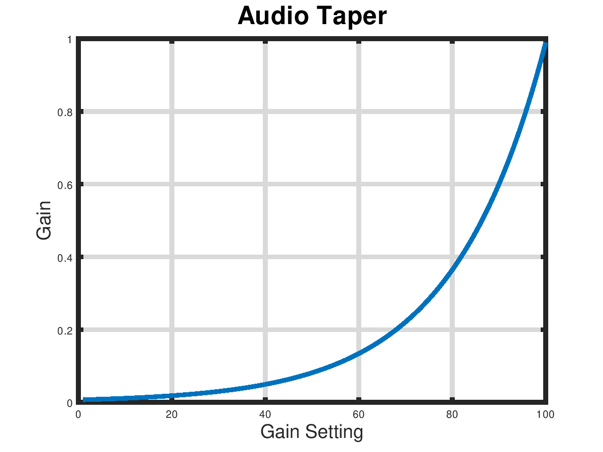 Square waves are easy to generate and have a pleasing sound since they have lots of higher harmonics. A more difficult question for a simple tone generator is how to control the volume. Human hearing perceives audio volume on a logarithmic scale. Electronics manufactures use what is called a 'audio taper' for potentiometers in audio applications. The diagram to the right shows an audio taper and we want our gain control to follow the same curve.
In this section the term 'gain' mean Vout/Vin where Vin the output voltage of the FPGA. Gain in this section is always between 0 and 1, and a lower gain means a lower volume.
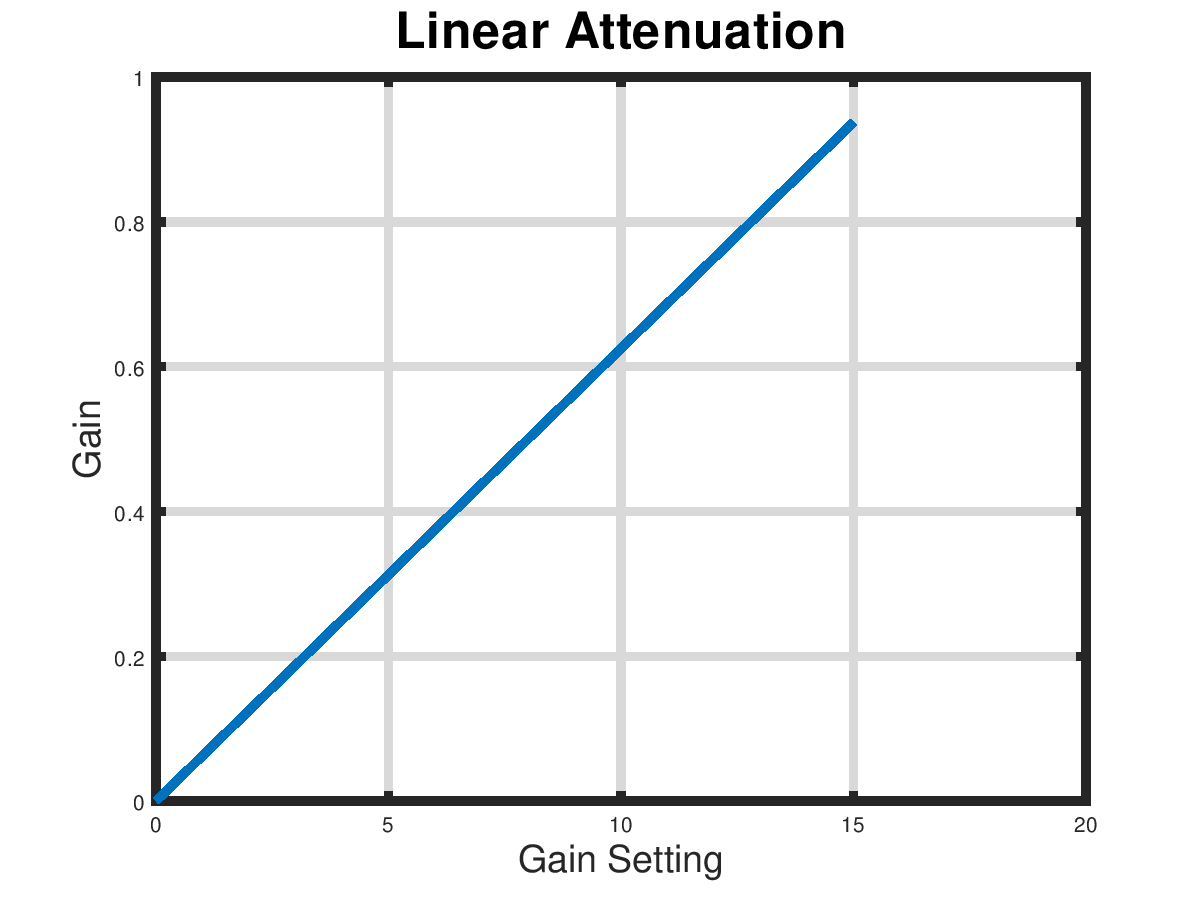
 There are two ways we can control the output volume of a square wave. The first is called 'pulse density modulation'. The idea is that we turn off the output briefly during the high part of the square wave. By briefly we mean fast enough that an RC low pass filter can easily average the fast pulses into a DC level during the high time of the square wave. In our case, we have two simple approaches to pulse density modulation. One is to have, say, a 4 bit counter run continuously at a high rate and to turn off the output if the count is less than a target (volume) value. The output volume is N/16 where N is a 4 bit value set by the host. This give a linear volume relative to N.
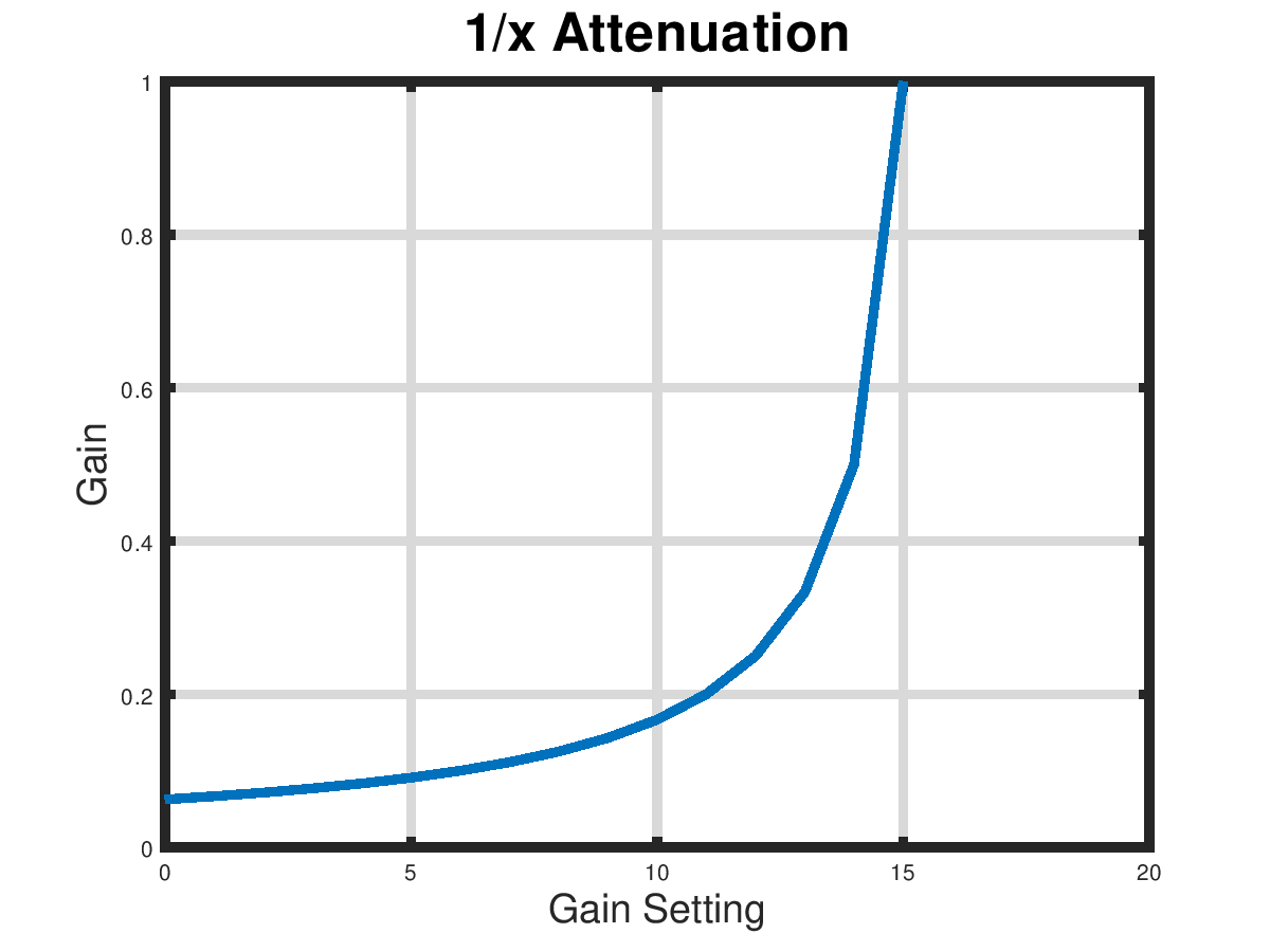
The other PDM method we can use is to output one pulse every N clock cycles. This gives a 1/N kind of response. Both linear and reciprocal approaches have about the same minimum and maximum attenuation and differ mostly in the intermediate values.
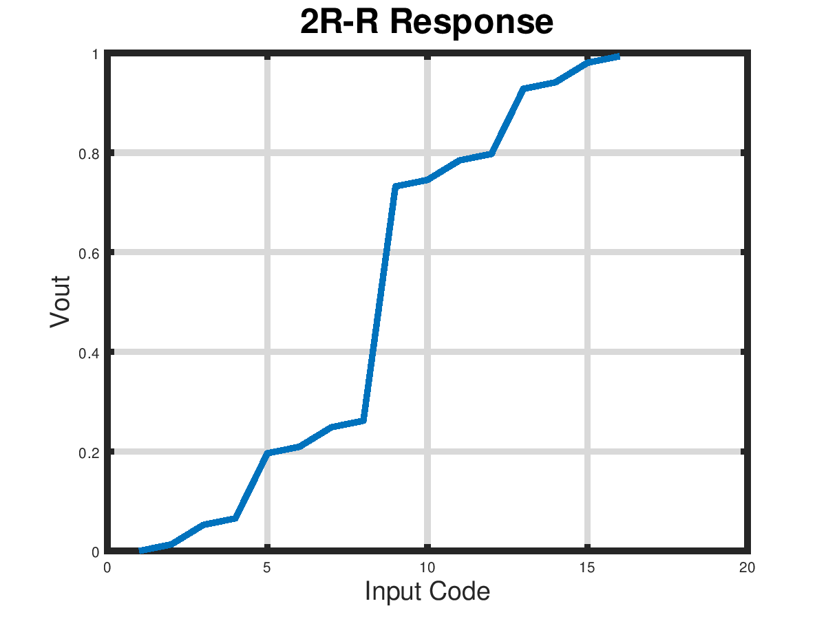
The other approach to volume control is to build a DAC out of resistors connected to the four FPGA pins dedicated to the peripheral. Many DACs use what is called an 'R-2R' resistor network of give a linear response to the input values. (See https://en.wikipedia.org/wiki/Resistor_ladder#R-2R) We specifically do not want a linear response. We want one in which the higher values are much greater than their linear equivalents. Shown below is a circuit that does this. In it we swap the normal linear R-2R network resistors to get a 2R-R resistor network. The gain of the circuit is clearly non linear.
The minimum output of the 2R-R circuit is 0.013 and the maximum value is 0.9935, a ratio of low to high of about 76. While we have lost a great deal of resolution, we have gone from 4 bits of dynamic range for the linear R-2R network to over 6 bits of dynamic range using a 2R-R network.
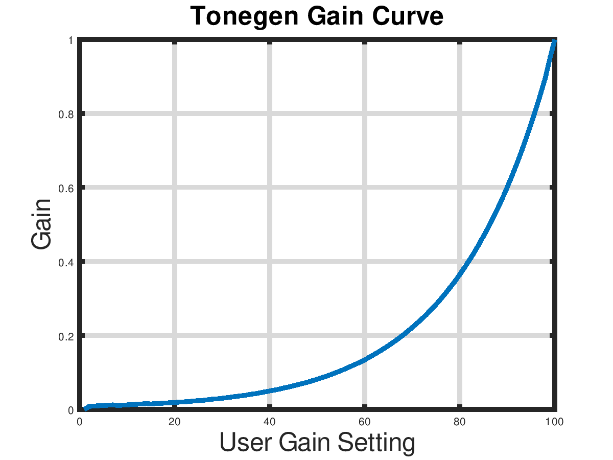 What if we combined the linear pulse density modulation with the non-linear DAC? We could PDM control each of the FPGA output pins with a separate 4 bit counter. Doing this gives 64K possible gain settings. Since some combinations give the same gain there are only 14000 unique gain settings. The minimum (one-sixteenth of the LSB) has a gain of 0.000817 and the maximum (all bits high) has a gain of 0.9314, giving us a dynamic range (log2(max/min)) of about 10 bits. This is not too bad considering we have a 4 bit DAC.
Our design is now ready for a Verilog Wishbone implementation. We should expect it to have a 24 bit phase accumulator, a 24 bit phase offset set by the host, four 4 bit PDM counters, four 4 bit gain settings set by the host, and an 8 bit duration counter (to count milliseconds),
(The diagrams in this section were generated using Octave. The sources are attached to this section in a wiki comment. Edit the page or contact the author to get the sources for the diagrams.)


