This is an old revision of the document!
Table of Contents
Baseboard4 User's Guide
Introduction
Thank you for your purchase of the Software Defined Peripherals (SDP) Starter Kit. This kit has everything you need to learn about software defined peripherals and to build a simple system using a set of peripherals that you choose.
Requirements
You should have some familiarity with the Linux command line and with programming in Python or C/C++. Prior experience with microcontrollers, robots, and simple wiring is very helpful. Although this kit is based on a field programmable gate array (FPGA) you do not need to know anything about FPGAs or circuit design. You will need a Linux computer that has a spare USB port. The computer can be a desktop, laptop, or a single board computer such as a Raspberry Pi. This kit contains a motor controller (called an H-bridge) but does not contain any motors. The H-bridge card is designed to connect directly to motors from Pololu but you can use any low voltage DC motors that you have available. The Pololu motors are: https://www.pololu.com/category/115/25d-metal-gearmotors
Overview
This document is broken into three major sections. The first section covers the theory of operation of software defined peripherals (SDP) and the Baseboard as an example. The second and largest section covers how to use the Baseboard. This section describes the API, how to order a set of peripherals for the Baseboard, and how to write a simple application using the Baseboard. We re-implement the simple application using ROS2. A third, more advanced section describes how to write your own software defined peripherals. This section covers both the driver and API as well as Verilog and circuit requirements. In the earlier sections we are careful to define the terms we use and explain ideas carefully. The later sections are more concise and will assume your Linux and programming experience.
Theory of Operation
What Are Software Defined Peripherals?
In the world of robotics and automation a peripheral is a device used for communication or for sensing and control. Communication peripherals include Inter-Integrated Circuit (I2C), Serial Peripheral Interface (SPI), asynchronous serial interfaces, and Ethernet interfaces. Counter and timer peripherals can implement pulse width modulation (PWM) for servo control and for DC motor control. Peripherals are generally hard-wired into the computer or microcontroller and can not be changed after the chip is built. Software defined peripherals are typically built on a Field Programmable Gate Array (FPGA). As the name implies, an FPGA has a huge array of gates and flip-flops. How the gates and flip-flops are interconnected is controlled by RAM that is set (or programmed) by the user (in the field). Software defined peripherals are built using gates, flip-flops, registers, and RAM. When you think of software, you probably think of lines of code executed in sequence on a Von Neumann CPU. FPGAs are not CPUs and do not execute sequential lines of code. Peripherals built using an FPGA use dedicated gates and registers designed to fill the intent of the peripheral. Many peripheral designers use schematics for their designs but a more common approach is to use a hardware description language such as Verilog or VHDL. In the same sense that HTML describes how to render a page, Verilog describes the interconnect of gates, registers, and external pins that make up a peripheral. The Verilog sources are compiled into a binary file that is loaded into the FPGA to implement the desired logic. Just as a PC has hardware that is independent of the OS loaded, so software defined peripherals must be divided into the hardware and the binary FPGA image. Your Baseboard4 is the hardware. DPcore is the FPGA image you load onto the Baseboard. We will refer to the FPGA binary in DPcore as the “SDP image” to make clear that it implements a set of software defined peripherals.
Architectures for Software Defined Peripherals
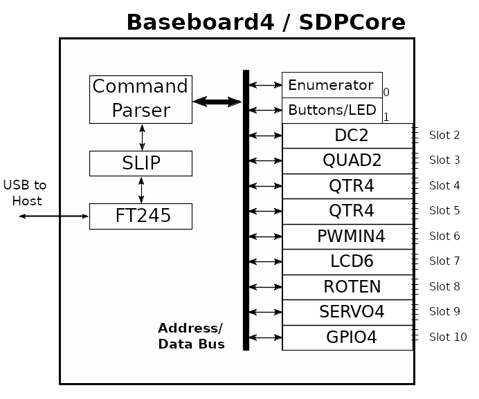 Figure 1 shows the internal architecture of DPcore with some typical peripherals. The areas in gray are built into every DPcore. The peripherals in white can change from one DPcore to the next. Later you will see how to build DPcore with your own selection of peripherals. Each peripheral is assigned a slot that has four dedicated FPGA pins. (Slot 10 has 3 pins.) The address bus in DPcore has 12 bits. The high 4 bits select the peripheral making the low 8 bits are available to the peripheral. Peripheral #0 is the enumerator, a read-only memory that has a list of the peripherals in the SDP image. At system start the host reads the enumerator to find what peripherals are available. The host can read and write peripherals on the bus by sending a command packet to DPcore. The command packet is decoded by the Command Parser and converted to read and write bus cycles. Commands can read or write to sequential addresses or can read or write to one address if a FIFO. Command packet are encapsulated using SLIP even though the packets are not IP packets.
Microcontroller peripherals are tightly coupled to the CPU and are accessed by the CPU over an internal address and data bus. Tightly coupling peripherals to the CPU has advantages and disadvantages. On the plus side you can get get much higher data rates with a closely coupled system. This might be important for image or video processing peripherals. Tightly coupled peripherals usually have an interrupt request line. This can be a problem for heavily loaded CPUs in which interrupts (and so data) can be missed or cause irregular sampling rates. The peripherals in DPcore are not closely coupled to a CPU and can not request service using an interrupt. Instead, most peripherals can be configured to automatically send data to the host when needed. Typically this might be for regular analog to digital conversion or when a monitored pin changes value. Polling is almost never needed with DPcore. One advantage of this is that your application can be entirely event driven if you wish.
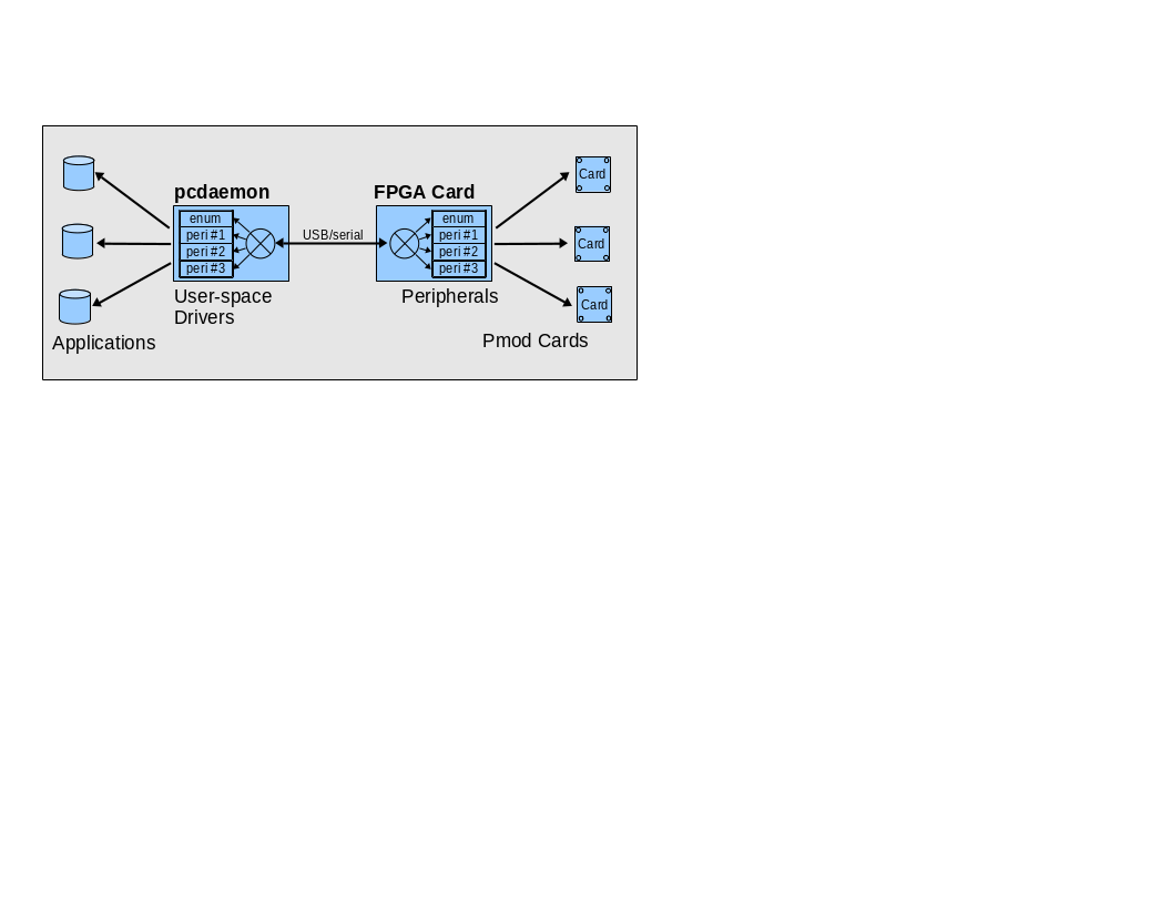 Figure 2 shows the architecture for a complete system. Peripherals share a common link between the Baseboard and the host. Dpdaemon is a program that runs on the host and provides the multiplexing and demultiplexing of data to and from the Baseboard. For every peripheral there is a corresponding user-space shared library, which we call a driver. Do not confuse our shared-object libraries for real Linux kernel drivers. We are using the term driver to mean the software that provides the API for the peripheral. When dpdaemon starts it reads the list of peripherals from the enumerator and loads the appropriate set of drivers. In this way the system responds automatically to whatever set of peripherals you load into DPcore.
Software Defined Peripherals on the Baseboard4
 In this section you will see how to connect your Baseboard4 to the other cards, how to select the peripherals you want in your system, how to generate an SDP image with those peripherals, how to load and run dpdaemon, and finally, how to use the API to test your system.
Physical Arrangement of Cards
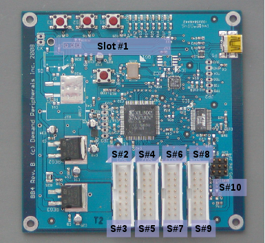
The Baseboard has four 16-pin connectors, each of which can support two different peripherals. Y-cables split the 16-pin connector into two 8-pin ones. Photo 1 shows the slot assignment for the connectors. Compare what you see in Photo 1 to what you saw in Figure 1. Slot numbers specifies a set of four pins on the Baseboard, and a peripheral number specifies the high four bits of the peripheral address. Slot numbers are always the same as peripheral numbers and we sometimes use the terms interchangeably.
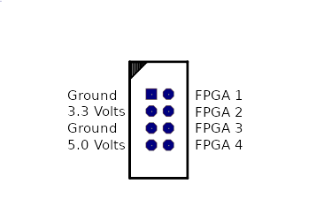 Some peripherals need eight FPGA pins and so use two slots. The octal servo controller and the octal IR proximity sensor are examples of an eight pin peripheral. However, most daughter cards have the 8-pin interface shown in Figure 3.
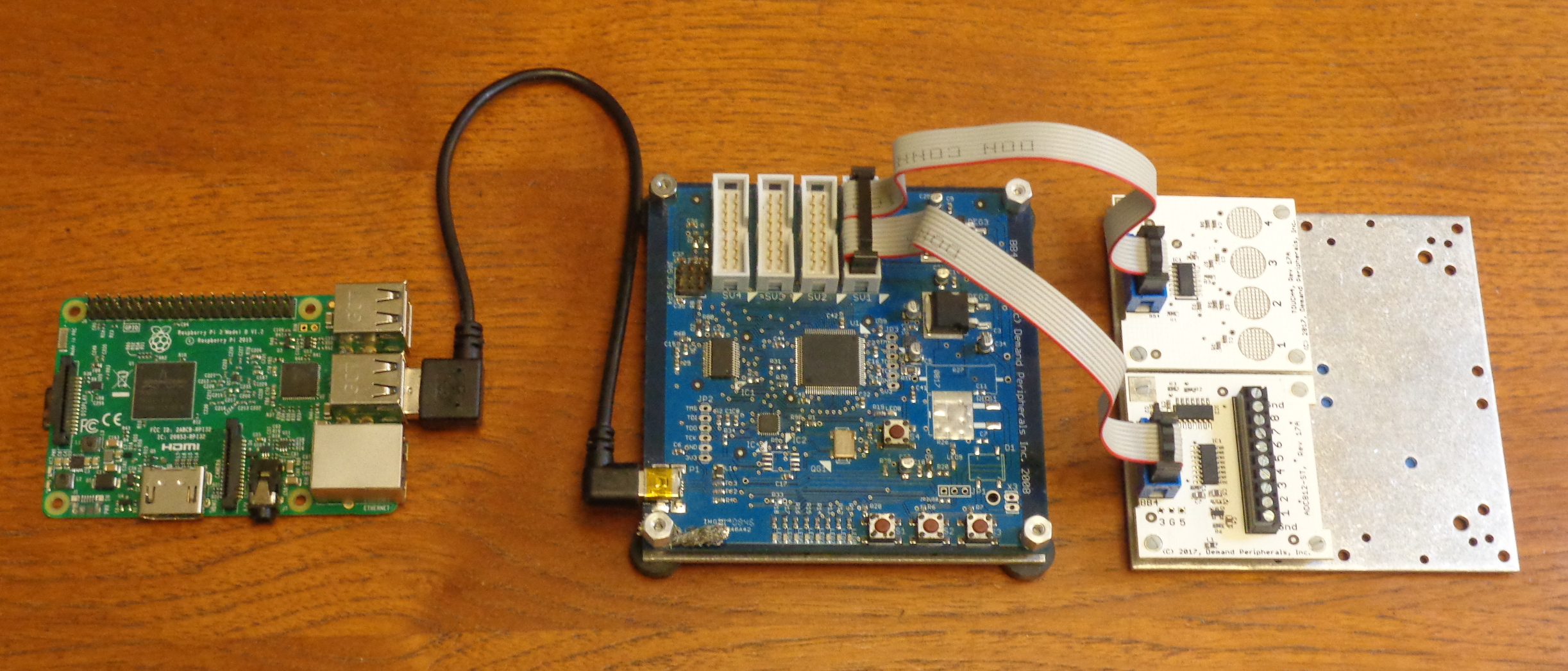
Photo 2 shows a host computer, a Baseboard, and a two daughter cards. Can you see that the quad touch sensor is in Slot 3 and the octal ADC is in Slot 2?
How to Generate a DPCore Binary
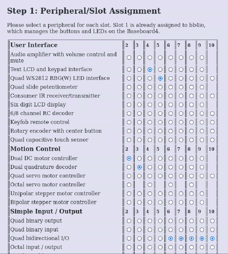
The easiest way to get an FPGA image is to use our web interface to ask us to build an image for you. Select Support and “Build your FPGA Image” to go to the Peripheral/Slot Assignment page. Figure 5 shows the top part of the slot assignment page. The peripherals are listed down the page and slots are listed across the page. Click the corresponding radio button to assign a particular peripheral to a slot. Figure 5 shows that a dual DC motor controller peripheral has been assigned to Slot #2.
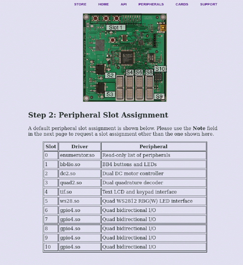
Figure 5 graphically illustrates one of the great advantages of software defined peripherals - any peripheral in any slot and they all work seamlessly. You no longer need to worry about pin conflicts, interrupt latency, or a VonNeumann bottleneck. The peripherals all have a Linux API, removing one more thing from your to-do list. After selecting peripherals for each slot press the Continue button at the bottom of the page. This takes you to a page where you can review and confirm your selection. This page also has a photo similar to Photo 1 above showing how the slot assignment map to the pins on the Baseboard.
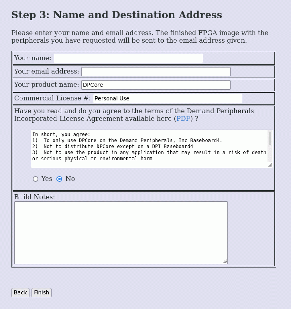
Click Continue on the review page to go to a page asking where to send the finished DPCore image. You will need to give name, email address, and accept the license. Figure 6 shows the page asking where to send the FPGA binary.
The name of the SDP image file is DPcore.bin and it should appear in your inbox the day after your request. The list of peripherals is prepended to the file and doing a ‘more’ on the file will show you its contents. The SDP image for the Starter Kit can be downloaded directly from
https://www.demandperipherals.com/downloads/StarterKit/DPCore.bin
If you wish to test building your own image for the Starter Kit please be sure to put the Dual DC Motor Controller Peripheral in Slot #2, the Dual Quadrature Decoder in Slot #3, and the Octal Pololu QTR Interface in Slot #4.
Loading and Running dpdaemon
The Baseboard connects to your computer using a USB-serial link. Data over the link consists of packets of binary data that read and write the registers in the software defined peripherals in DPCore. Your high level application could communicate with the Baseboard directly but almost everyone finds it easier to deal with an API that translates high-level API commands into read and write packets to the Baseboard. Dpdaemon provides this easy to use API for your applications. You can download and install dpdaemon with the following commands:
    git clone https://github.com/DemandPeripherals/dpdaemon.git
    cd dpdaemon
    make
    sudo make install
The Baseboard has an FTDI USB-to-serial interface. Connect the Baseboard to your computer and determine the name of the serial port. Start dpdaemon with the command:
dpdaemon -l /usr/local/lib/DPCore.bin -s /dev/ttyUSB0
You can perform a quick test that everything is working by changing the LEDs on the Baseboard with the command:
/usr/local/bin/dpset bb4io leds 55
Dpdaemon is a true daemon in that, by default, it will disassociate from the controlling terminal, respawn itself, and use syslog() to report errors. You can change this behavior with the -f command line option. This keeps the daemon in the foreground. The -e command option tells the daemon to not use syslog() and to report errors to the controlling terminal. The API to dpdaemon uses ASCII commands over a TCP link. The TCP listen port has a default of 8870. You can override this default with the -p command line option. Dpdaemon monitors only one serial port. You can use an alternate TCP port if you ever want to run two instances of dpdaemon connected to two different serial ports. The -a option tells the daemon to listen on any IP interface not the default of 127.0.0.1. While a security risk, listening on any network interface can be handy when the high level application runs on a separate computer. The -l option tells the daemon which binary image to load onto the FPGA at startup. There is no default image. The -s option specifies which serial port to use. The default is /dev/ttyUSB0. Many Linux systems support real-time extensions to the job scheduler. You can invoke these extensions for dpdaemon using the -r command line option. The drivers to load when dpdaemon starts are specified in the enumerator peripheral. You can override what driver is loaded using the -o option. Running dpdaemon with the -h option give the following help text:
  dpdaemon [options]
  options:
  -e, --stderr       Route messages to stderr instead of log even if
                     running in background (i.e. no stderr redirection).
  -v, --verbosity    Set the verbosity level of messages: 0 (errors), 1
                     (+debug), 2 (+ warnings), or 3 (+ info), default = 0.
  -d, --debug        Enable debug mode.
  -f, --foreground   Stay in foreground.
  -a, --listen_any   Use any/all IP addresses for UI TCP connections
  -p, --listen_port  Listen for incoming UI connections on this TCP port
  -r, --realtime     Try to run with real-time extensions.
  -V, --version      Print version number and exit.
  -o, --overload     Load .so driver file for slot, as slotID:file.so
  -h, --help         Print usage message.
  -s, --serialport   Use serial port specified not default port.
  -l, --load         Load DPCore.bin specified.
It is easy to start dpdaemon in your rc.local or other start up file with the following command:
/usr/local/bin/dpdaemon -l /usr/local/lib/DPcore.bin
Of course the above will need to match where you install dpdaemon and your SDP image file.
The next section describes the dpdaemon API. We believe that the simple API offered by dpdaemon is suitable for all types of simple automation such as vending machines, automatic cat doors, and two-wheeled robots. However, the dpdaemon API is just one of many possible APIs. You could, for example, replace dpdaemon with a g-code interpreter if you wanted to to build a 3-axis machine tool, or you could replace the loadable driver modules of dpdaemon with their equivalent ROS2 nodes.
The dpdaemon API
Resources
A resource is an application visible name given a configuration parameter or a sensor value. For example, the buttons and LEDs on the FPGA card are are in the “bb4io” peripheral and have resource names of “buttons” and “leds” respectively. Resources can be read-write, write-only, or read-only depending on the nature of the resource. Most configuration resources are read-write, and sensor reading are usually read-only. Some sensor resources can be configured to automatically send a reading only when the input changes or when a timer expires. This can greatly simplify your application since you do not need to continuously poll sensors to detect changes. The Peripherals section of the Demand Peripherals web site gives a detailed description of the meaning and use of the resources for each peripheral. You can also get help on a peripheral's resources using the dplist command described below.
API Commands
The API has five commands. You can set a resource, such as a configuration parameter. You can get a resource, such as a status value. You can cat a resource, such as a stream of sensor data. Two more commands let you list the peripherals in the system and load a driver module not included in the enumerator. The commands are all ASCII text terminated by a newline over a TCP connection. Resource values are also given as ASCII text. Dpdaemon will send back an error message if the command was not recognized and a single backslash character after the command has been processed. The commands have the following syntax:
      dpset <slot#|peri_name> <resource_name> <value>
      dpget <slot#|peri_name> <resource_name>
      dpcat <slot#|peri_name> <resource_name>
      dplist [peri_name]
      dploadso <full path to .so driver file>
Dplist lists the driver modules loaded by dpdaemon. Giving dplist the name of a peripheral returns a page of help text and examples for that peripheral. Note that when you have more than one instance of a peripheral in the system you must use the slot number to address instances other than the first one. One of the things we like about the dpdaemon API is that the commands all look like Linux command line commands. In fact, while the underlying protocol is still TCP based, all of these command have bash command line equivalents. This means you can easy view, test, or configure your system from the command prompt.
EXAMPLES: The FPGA card has buttons and LEDs that are visible from the API.
      dpset bb4io leds ff   # turn all LEDs on
      dpcat bb4io buttons   # wait for a button press
The dual DC motor controller peripherals, dc2, has controls for the PWM frequency, the mode (forward, reverse, brake, or coast), the PWM duty cycle, and a watchdog timer that stops the motors if there are no speed updates within a certain time.
      dpset dc2 pwmfrequency 20000    # set PWM freq to 20KHz
      dpset dc2 mode0 f     # motor 0 in forward mode
      dpset dc2 mode1 f     # motor 1 in forward mode
      dpset dc2 watchdog 15 # watchdog set to 1.5 seconds
      dpset dc2 power0 40   # motor 0 at 40% PWM
      dpset dc2 power1 70   # motor 0 at 70% PWM
The 6 digit LCD display peripheral, lcd6, lets you control individual segments or output fully formed digits.
      dpset lcd6 display 1234.56 # display a number
      dpget lcd6 segments        # ask which segments are on
The octal 12-bit analog-to-digital peripheral, adc812, lets you specify the sample rate and whether or not to combine two inputs into one differential input ADC channel.
      dpset adc812 config 25, 0x00  # 25 ms updates, all singled ended
      dpcat adc812 samples   # start sample stream
A Sample Program
The following is a simple but complete Python program that shows how to use the dpdaemon API. The source code is available http://demandperipherals.com/downloads/counter.py
  #!/usr/bin/env python
  import socket
  import sys

  # This program opens two sockets to the dpdaemon, one
  # to listen for button press events and one to update
  # the LED display.  This code uses a blocking read but
  # a select() implementation would work too.
  #
  # Pressing button 1 increments the count, button 2
  # clears the count and button 3 decrements the count.
  # Buttons are represented as hex values 1, 2, and 4.

  # Global state information
  count = 0

  try:
      sock_cmd = socket.socket(socket.AF_INET, socket.SOCK_STREAM)
      sock_cmd.connect(('localhost', 8870))
      sock_button = socket.socket(socket.AF_INET, socket.SOCK_STREAM)
      sock_button.connect(('localhost', 8870))
      sock_button.send('dpcat bb4io buttons\n')
      # loop forever getting button presses and updating the count
      while True:
          display_count = count
          if display_count < 0:
              display_count = count + 256
          sock_cmd.send('dpset bb4io leds ' "%x" '\n' % display_count)
          key = sock_button.recv(6)
          keyint = int(key[:3])
          if keyint == 1:
              count = (count + 1) % 256
          elif keyint == 2:
              count = 0;
          elif keyint == 4:
              count = (count - 1) % 256

  except KeyboardInterrupt:
      # exit on Ctrl^C
      sock_cmd.close()
      sock_button.close()
      sys.exit()

  except socket.error:
      print "Couldn't connect to dpdaemon"
      sys.exit()
Build a Robot Using a Baseboard4
Use ROS2 to Control Your Robot
How to Write a Custom Driver for dpdaemon
A Brief Introduction to Verilog
In this section you will see how to use Verilog to build FPGA applications. The purpose of this section is to give non-Verilog users a sense of how Verilog works. This is an advanced section and is entirely optional. To appreciate this section you should already be familiar with digital circuit design. This section is broken into four topics:
- “hello world” in Verilog
- use iverilog to test your Verilog circuit
- install the Xilinx compiler
- compile your design and test it on the Baseboard
"Hello World" in Verilog
Most programming languages have a sample application that prints the phrase “Hello, World!” to the console. This application is often used to validate the installation of the language and its tool chain. For microcontrollers and FPGAs the equivalent application usually flashes an LED on the development board. The Verilog program below implements a counter on the Baseboard LEDs. Save the following as counter.v
  // Simple up counter for the Baseboard.
  // Visible update rate is about 12 times per second

  module counter(CK12, LEDS);
      input   CK12;        // 12.5 MHz input clock
      output  [7:0] LEDS;  // eight LEDs on Baseboard

      reg [27:0] count;    // 28 bit counter

      initial
      begin
          count = 0;
      end

      always @(posedge CK12)
      begin
          count <= count + 28'b1;
      end

      assign LEDS = count[27:20];   // display high 8 bits of counter

  endmodule
Bob: do a code review of the above and be sure to describe wire, reg, assign and “⇐”
Test you Verilog design using iverilog
Bob: describe why you'd want to do simulation
Install iverilog and gtkwave on a Debian system with the command:
sudo apt-get install iverilog gtkwave
Bob: describe how a test bench works in iverilog
Save the following as counter_tb.v
  //  iverilog test bench for the simple counter in counter.v

  `timescale 10ns/10ns

  module counter_tb;
      // direction is relative to the DUT
      reg    clk;          // 12.5 MHz system clock
      wire   [7:0] leds;   // LEDs on Baseboard

      // Add the device under test
      counter counter_dut(clk, leds);

      // generate the clock
      initial  clk = 0;
      always   #4 clk = ~clk;  // half period is 40ns == 4 * timescale

      initial
      begin
          $dumpfile ("counter_tb.xt2");
          $dumpvars (0, counter_tb);

          // 100 million steps of 10ns is one tenth of a second
          #100000000
          $finish;
      end
  endmodule
Run the simulation, convert the output to a gtkwave format, and display the results with the commands:
  iverilog -o counter_tb.vvp counter_tb.v counter.v
  vvp counter_tb.vvp -lxt2
  gtkwave counter_tb.xt2
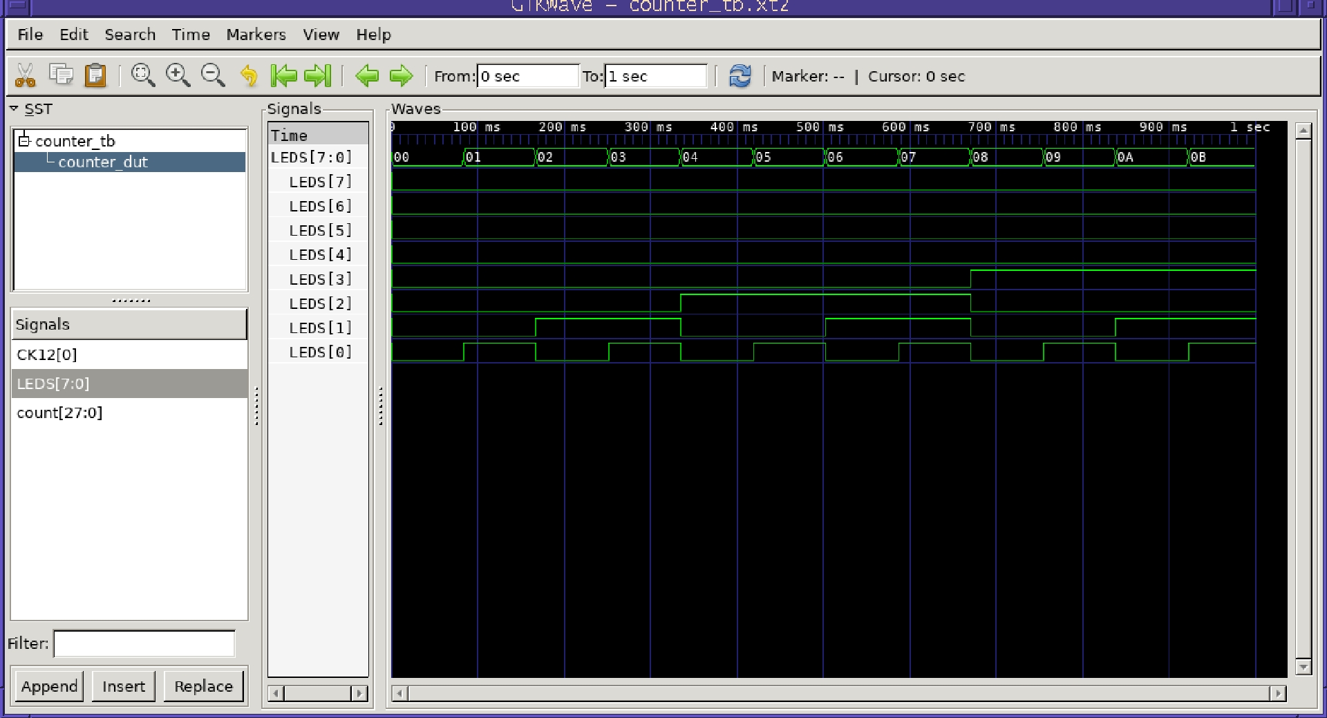
To view the LED waveforms click on “counter_tb” and “counter_dut” in the top left gtkview pane. Then click on “LEDS” in the lower left pane. Double click on “LEDS” in the display pane to expand the eight lines. Hold down the CTRL key and use the mouse scroll wheel to compress the display until the whole second of simulation is displayed. The display should look something like this:
Install and Test the Xilinx Toolchain
Once your simulation output is correct you are ready to compile and download your design to the FPGA. This section describes how to install the Xilinx FPGA design tools, how to use the Xilinx command line tools to compile a Verilog design, and how to download the compiled code to the Baseboard. A later section will describe how to automate all these steps in a Makefile.
The Baseboard uses a Xilinx Spartan-3E and a USB interface for both downloads and a host interface. Since the Baseboard is downloaded through a USB serial port you do not need a JTAG cable or dongle.
Xilinx provides a set of free design tools, ISE, which are part of their WebPACK download. To get the WebPack download you have to select it, register with Xilinx, and start the download.
Start by going to the Xilinx download site at: http://www.xilinx.com/support/download/index.htm. Click on “ISE Archive” link and select “14.7” and then “Full Installer for Linux”. This will take you to a login page where you can select “Create Account” (since you probably don't already have a Xilinx account). You activate the account using a token sent in email. Your first login will present a page asking you to verify your name and address. The download starts automatically after selecting Download at the bottom of the name verification page.
Install the software by untarring the download file and running the “xsetup” script in the top level directory. If installing as a non-root user, you might want to create /opt/Xilinx/14.7 beforehand and give yourself write permission on it.
The installation will ask which products to install. We suggest the “ISE WebPACK” as it is the smallest and has everything you'll need. You need to “Acquire or Manage a License Key” but you do need to install the Cable Drivers. Selecting Next then Install should start the installation.
Once the installation is complete you can add the Xilinx Verilog compiler toolchain to you path and verify that it can be found with the commands:
  export PATH=$PATH:/opt/Xilinx/14.7/ISE_DS/ISE/bin/lin64
  which ise
By default, ise opens a graphical integrated development environment. DPcore is make based and you do not need to learn the IDE. You may recall that compiling a C++ or C program is broken into the steps of preprocessing, compiler pass 1, compiler pass 2, assembly, and linking. All these steps occur even though you only type g++ or gcc. In the same way, Verilog is compiled to binary in several steps.
Before compiling your Verilog to an FPGA binary you need to tell the compiler how the wires in the Verilog module map to the physical FPGA pins. Xilinx uses a “user constraints file” (.ucf) for this. The minimum UCF file for your counter is shown below. Save it as counter.ucf
  NET "CK12"      LOC = "P39"  ;    # 12.5 MHz clock
  NET "LEDS[0]"   LOC = "P70"  ;    # LED 0
  NET "LEDS[1]"   LOC = "P71"  ;    # LED 1
  NET "LEDS[2]"   LOC = "P62"  ;    # LED 2
  NET "LEDS[3]"   LOC = "P66"  ;    # LED 3
  NET "LEDS[4]"   LOC = "P67"  ;    # LED 4
  NET "LEDS[5]"   LOC = "P68"  ;    # LED 5
  NET "LEDS[6]"   LOC = "P63"  ;    # LED 6
  NET "LEDS[7]"   LOC = "P65"  ;    # LED 7
The commands that Xilinx uses to compile Verilog for a SPartan3 can be hidden by a Makefile but you might be interested in the steps involved. There is insufficient space in this tutorial to give detailed descriptions of the commands. Your download of the Xilinx tools includes comprehensive manuals for the Xilinx command line tools which you can consult if you are interested. Look in ISE/doc/usenglish/books/docs/. The following paragraphs give a brief overview of the commands involved.
The first command, xst, synthesizes the Verilog file into a hardware design that is saved as a netlist file with an .ngc extension. Xilinx's xst program is actually a command line interpreter and it expects input from standard-in. Use an echo command and a pipe operator to give xst input from standard-in if you want to keep all of your build information in a Makefile.
echo "run -ifn counter.v -ifmt Verilog -ofn counter.ngc -p xc3s100e-4-vq100" | xst
You have to specify the input file, the input file format, the name of the output file and the exact type of FPGA. Xst generates several report files and directories, but the real output is a netlist file with an .ngc extension that is required for the next command. You can examine the output files and reports to better understand the how the synthesis works and an appendix in the xst manual describes the output files and reports in detail.
The ngdbuild command further decomposes the design into FPGA native elements such as flip-flops, gates, and RAM blocks.
ngdbuild -p xc3s100e-4-vq100 -uc counter.ucf counter.ngc
It is the ngdbuild command that first considers the pin location, loading, and timing requirements specified in the user constraints file, counter.ucf. Like the other Xilinx commands, ngdbuild produces several reports but its real output is a “Native Generic Database” stored in a .ngd file.
The Xilinx map command converts the generic elements from the step above to the elements specific to the target FPGA. It also performs a design rules check on the overall design. The map command produces two files, a Physical Constraints File file and a Native Circuit Description file, that are used in subsequent commands.
map -detail -pr b counter.ngd
The map command produces quite a few reports. As you gain experience with FPGA design you may come to rely on these report to help identify design and timing problems.
The place and route command (par) uses the Physical Constraints File and the Native Circuit Description to produce another Native Circuit Description file which contains the fully routed FPGA design.
par counter.ncd parout.ncd counter.pcf
Output processing starts with the bitgen program which converts the fully routed FPGA design into the pattern of configuration bits found in the FPGA after download.
bitgen -g StartUpClk:CClk -g CRC:Enable parout.ncd counter.bit counter.pcf
The bitgen program lets you specify which clock pin to use during initialization and whether or not to generate a CRC checksum on the download image. Files which contain a raw FPGA download pattern are called bitstream files and traditionally has a .bit file extension. Bitstream files are good for downloads using JTAG but since we're downloading over a USB serial connection one more command is required to convert the bitstream file into a download file.
promgen -w -p bin -o counter.bin -u 0 counter.bit
The promgen program is a utility that converts bitstream files into various PROM file formats. The format for the Baseboard is called bin so the promgen command uses the -p bin option. The output of promgen, counter.bin, is what you download to the Baseboard FPGA card.
All of the commands described above, including xst, ngdbuild, map, par, bitgen, and promgen have excellent PDF manuals in either the ISE/doc/usenglish/books/docs/xst directory or the ISE/doc/usgnglish/de/dev directory of your WebPACK installation.
  echo "run -ifn counter.v -ifmt Verilog -ofn counter.ngc -p xc3s100e-4-vq100" | xst
  ngdbuild  -p xc3s100e-4-vq100 -uc counter.ucf  counter.ngc
  map -detail -pr b counter.ngd
  par counter.ncd parout.ncd counter.pcf
  bitgen -g StartUpClk:CClk -g CRC:Enable parout.ncd counter.bit counter.pcf
  promgen -w -p bin -o counter.bin -u 0 counter.bit
When the Baseboard powers up or after pressing the reset button the FPGA waits for an binary image from the serial port. Linux serial port drivers can suppress certain characters from an output stream. To prevent this you need to turn off post processing on the serial port.with the command:
sudo stty --file=/dev/ttyUSB0 -opost # We want raw output
Press the reset button and send the FPGA binary to the Baseboard with the command:
cat counter.bin > /dev/ttyUSB0
If all has gone well you should see an up counter on the Baseboard LEDs.
How to Write a Wishbone Peripheral
In this section you will see how to build your own custom Verilog peripheral. This is an advanced section and is entirely optional. To appreciate this section you should already be familiar with digital circuit design and Verilog. This section is broken into five topics:
- the DPcore Wishbone bus
- build a Verilog peripheral for DPcore
- fold your peripheral in the DPcore build system.
The Wishbone Bus
A Wishbone Bus is a synchronous, parallel data bus intended to connect on-chip peripherals to an on-chip CPU. Wishbone describes both the interface signals to the peripherals as well as the how the peripherals are connected to each other and to the CPU. The full specification is at Wishbone specification. Wishbone is a common interface for many of the project at Opencores.
In the case of DPcore, the Wishbone bus does not connect to a CPU but to an interface to a host computer.
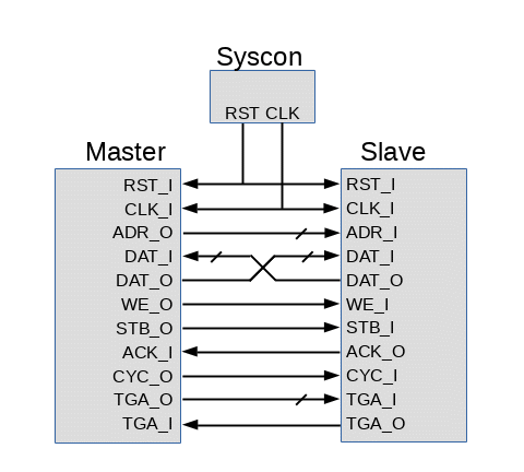
Wishbone supports different peripherals/CPU interconnect topologies. You may already be familiar with a shared bus topology since early PCs used these as the ISA and PCI buses. A crossbar topology is often used when peripherals need to communicate amongst themselves or with a DMA controller. A point-to-point topology is often used when the bandwidth requirements of a peripheral would interfere with access to other peripherals. A ring topology is often used when speed is less important than the amount of FPGA fabric used in the system. DPcore uses a ring topology. Note that the topology does not necessarily affect the address, data, and control lines going to and from the peripheral. The diagram to the right shows the major Wishbone signals in a point-to-point topology.
Wishbone gives a general description of a peripheral bus. For example, Wishbone buses can be 8, 16, 32, or 64 bits wide. It is up the the implementer to decide things like bus width, clock frequencies, and which controls lines to use. The Wishbone specification lists and defines both required and optional bus signals.
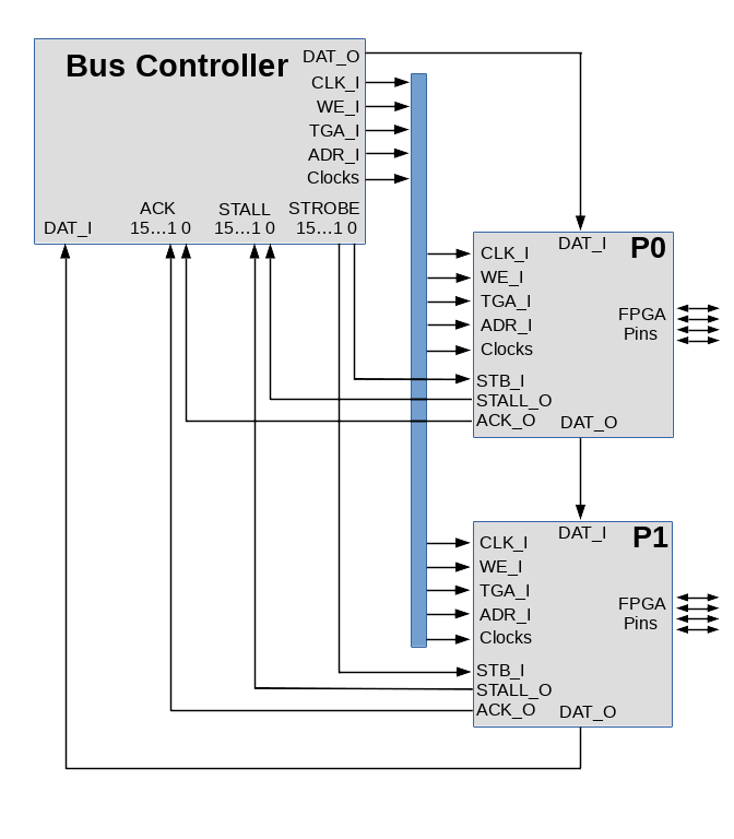
The diagram to the right shows the topology for PDcore. It shows two of the possible sixteen peripherals. The DPcore data bus is 8 bits wide. Each peripheral has 8 bits of internal addressing. That is, each peripheral can have up to 256 8-bit registers. You have previously seen that one advantage of DPcore is that you can have any mix of peripherals you want. This diagram illustrates why. All peripherals have the same interface, so any peripheral can be substituted for any other.
The paragraphs below describe the Wishbone bus as implemented for DPcore. We use _X to indicate both input (_I) and output (_O) signals. Instead of the terms Master and Slave we use the term Controller and Peripheral which better match our use of Wishbone. In our implementation when a peripheral is not selected it must route DAT_I to DAT_O unchanged–.
Peripheral Signal Names : CLK_I : System clock. All peripherals use this 20 MHz clock to drive state machines and other peripheral logic. This is used by the controller and all peripherals.
WE_I : Write enable. This is set to indicate a register write into the peripheral. A zero for WE_I indicates a read operation.
STB_I : Strobe. This is set to indicate that a bus cycle to this peripheral is in progress. The cycle can be either a register read/write or a poll.
TGA_I : Address tag. A bus cycle with TGA_I set is a normal register read/write. For a read bus cycle with TGA_I cleared, the peripheral places the number of bytes it wishes to send to the host on DAT_O. A DAT_O value of zero indicates that the peripheral has no data for the host at this time. If DAT_O is non-zero the controller internally generates a read request for the number of bytes specified.
ADR_I : Address. An 8 bit address that specifies which register in the peripheral to read or write. The peripheral can treat some addresses as simple register reads/writes and other addresses as top-of-stack for a FIFO.
STALL_O : Stalled. The peripheral asserts this signal to indicate that more system clock cycles are needed to complete the bus cycle. The controller waits for STALL_O to be deasserted before completing the read or write operation.
ACK_O : Acknowledge. The peripheral asserts ACK_O to tell the controller that the read or write bus cycle has successfully completed. This signal is used in FIFO accesses to indicate that a FIFO is full (on write) or empty (on read). The controller write successive bytes to the same address to fill a FIFO. As long as the bytes are successfully written, the peripheral asserts ACK_O. When a byte can not be written, the peripheral does not raise ACK and the controller knows that the FIFO is full and the sequence of writes stops at that point. The controller sends an acknowledgment to the host giving the number of bytes written (or read). This lets the host application know how many bytes were successfully written to the FIFO letting the application resend the unacknowledged bytes at a later time.
DAT_X : An 8 bit data bus that is passed in ring from the bus controller through all peripherals and back to the bus controller. This arrangement is close to the Wishbone Data Flow Interconnection but the data path is a ring. This arrangement is sometime called a “serpentine” bus. The “Port Size” is 8 bits and the “Granularity” is 8 bits. There is no “Endianness” associated with the data bus. During a bus write cycle the peripheral latches DAT_I into the selected register. During a read bus cycle the peripheral ignore DAT_I and places the requested data on DAT_O.
The Verilog code fragment below shows a typical peripheral interface definition. “Clocks” are system available strobes that occur every 100ns, 1.0us, 10us, 100us, 1.0ms, 10ms, 100ms, and 1 second. The four inout pins go to the FPGA pins. Some peripherals have eight instead of four FPGA pins.
module dp_peri(CLK_I,WE_I,TGA_I,STB_I,ADR_I,STALL_O,ACK_O,DAT_I,DAT_O,clocks,pins);
    input  CLK_I;            // system clock
    input  WE_I;             // direction. Read-from-peri==0; Write-to-peri==1
    input  TGA_I;            // ==1 for register read/write, ==0 for data-to-send poll
    input  STB_I;            // ==1 if peri is addressed for r/w or poll
    input  [7:0] ADR_I;      // address of target register
    output STALL_O;          // ==1 if we need more clk cycles to complete
    output ACK_O;            // ==1 if we claim the address and complete the read/write
    input  [7:0] DAT_I;      // Data INto the peripheral;
    output [7:0] DAT_O;      // Data OUTput from the peripheral, = DAT_I if not us.
    input  [7:0] clocks;     // 100ns to 1 second pulses synchronous CLK_I
    inout  [3:0] pins;       // FPGA pins for this peripheral
The DPcore implementation of Wishbone is fairly bare-bones. That is, it does not use other Wishbone signals such as: RST_I, TGD_I, TGD_O, CYC_I, ERR_O, LOCK_I, RTY_O, SEL_I, or TGC_I.
Download, Build, and Test DPcore
You can download the source code for DPcore and build a binary image with the following commands:
      git clone https://github.com/DemandPeripherals/DPCore.git
      cd DPCore/src
      # Edit perilist to set the peripherals in your build
      vi perilist
      make
Expect several warnings about signals without loads. This happens because some pins are defined but never used.
      sudo cp DPCore.bin /usr/local/lib
      # start dpdaemon and test Baseboard LEDs
      dpdaemon -l /usr/local/lib/DPCore.bin -s /dev/ttyUSB0
      /usr/local/bin/dpset bb4io leds 55

